




CNC Semiconductor Parts Applications in Wafer Processing
CNC semiconductor parts are essential for current chip processing because they provide the micron-level accuracy needed for making semiconductors. These precision-machined parts make it possible to handle them without getting them dirty, to line them very precisely, and to get solid performance in etching, casting, and testing settings. Dongguan Junsion Precision Hardware Co., Ltd. makes parts with tolerances of up to ±0.01mm. Our advanced multi-axis CNC cutting and strict quality standards help global chip makers get consistent results and reduce costly downtime.
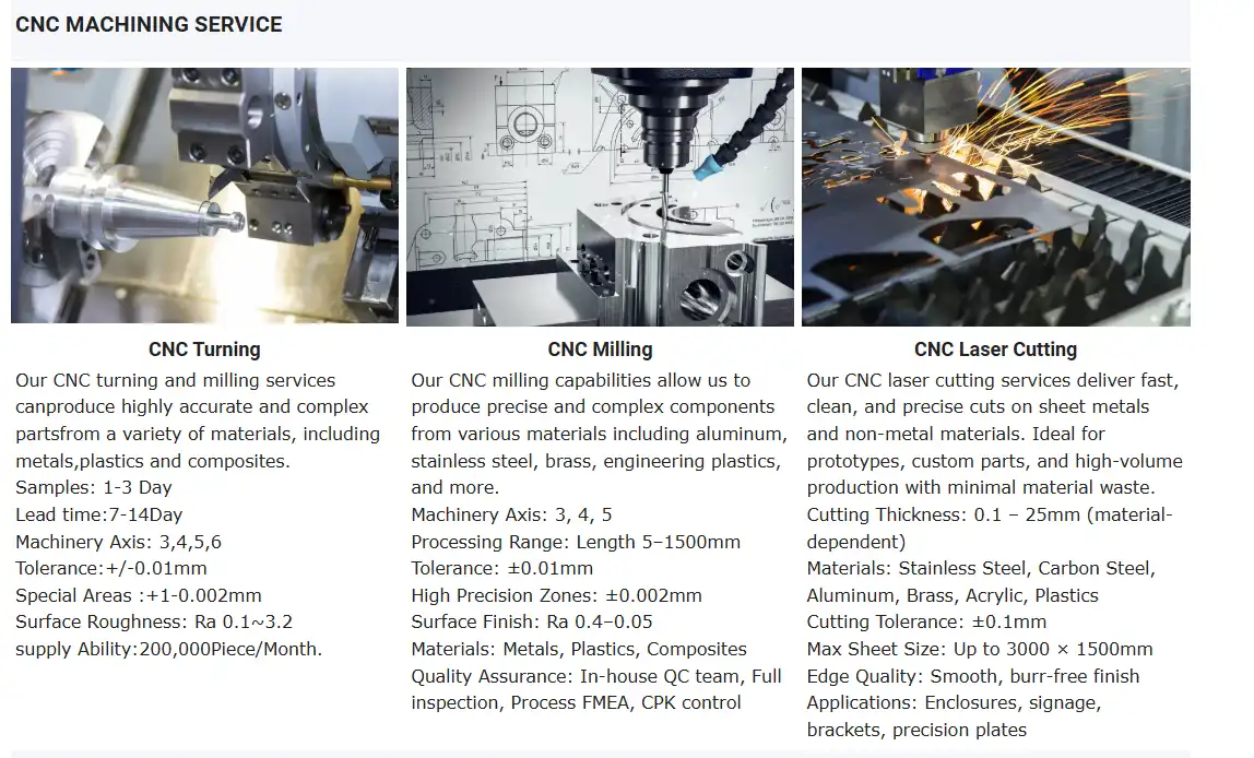
Understanding CNC Semiconductor Parts and Their Role in Wafer Processing
Precision-machined parts are an important part of every step in the process of making a semiconductor chip. CNC semiconductor parts are different from regular-made parts because they need to be very accurate in terms of size and surface quality. For general industry uses, traditional cutting might be enough. But for semiconductor tools, tolerances must be measured in microns, and the surface must be smooth and free of tiny flaws that could damage the chip surfaces.
Material Selection for Semiconductor Environments
The hard conditions of factories that make semiconductors mean that strict material standards must be met. Extreme temperature changes, plasma gases that are bad for electronics, and an ultra-high vacuum are all things that wafer processing equipment has to deal with. Materials need to be able to withstand chemical attacks and keep their shape at all temperatures, from very low temperatures to high temperatures used for processing. High-purity aluminium alloys, such as 6061-T6 and 7075, have great strength-to-weight ratios and can transfer heat well, making them useful for uses that need to cool things down. Grades 316L and 304 stainless steel are better at resisting rust in chemical distribution systems and wet processes. Titanium alloys are the most chemically stable materials that can be used in plasma etching tanks and reactive ion etching tools. High-performance industrial plastics, like PEEK and POM, are used in specific situations where keeping electricity safe or reducing particle production is very important.
Advanced Manufacturing Processes
From a raw material to a finished semiconductor component, a lot of complex CAD/CAM code is needed to turn engineering requirements into exact toolpath strategies. Multi-axis CNC tools can make complicated shapes that would be hard to make by hand or by casting. Our factory has 32 high-tech CNC tools that can work on five axes at the same time. This lets us make complex cooling channels, undercut features, and compound-angle surfaces all in one setting. This method cuts down on wait times while getting rid of mistakes that build up over time from doing multiple tasks. Coordinate measuring machine (CMM) checking, surface profilometry, and visual comparisons against CAD models are some of the ways that quality is checked at different steps of production.
Advantages Over Traditional Manufacturing
CNC methods are repeatable, which means that every part meets specs within very small error bars. CNC cutting allows for fast testing and design tweaks, while injection moulding needs expensive equipment investments and long wait times for design changes. When equipment specs change, it's helpful for the buying manager to be able to change sizes or features between runs of production without having to pay for retooling. Because CNC code is digital, it allows version control and tracking, which are important for semiconductor quality management systems that meet SEMI standards and ISO certifications.
Applications of CNC Semiconductor Parts in Wafer Processing Equipment
Wafer processing is made up of dozens of steps that happen one after the other. Each step needs special parts that keep the process running smoothly and can handle practical pressure. Precision-machined elements are used at every step of the manufacturing process, from adding the base to checking the end product.
Wafer Handling and Transport Systems
Controlling contamination is the most important thing in chip handling processes. Killer flaws that stop chips from working can be made by particles as small as a nanometre. Our precisely made chip handle parts have surface finishes that get Ra values below 0.2 microns, which reduces the sticking and formation of particles. Anodising processes make the sides of end effector blades made of aluminium alloys hard and immune to wear. They also provide electrical grounding to get rid of static charges. To keep their positional accuracy over millions of transfer cycles, robotic arm links need to have very small error margins. Edge grippers and vacuum chucks control the amount of force that contacts the edges of the chip. This stops stress-induced micro-cracks and keeps substrates in place during high-speed motions.
Etching and Deposition Tool Components
Aggressive fluorine and chlorine radicals are energized in plasma etch chambers, bombarding interior components. For CNC Semiconductor parts used in these environments, specialized materials must be employed for electrode plates, gas distribution plates, and confinement rings to resist chemical attack and maintain dimensional stability. Our etch tool components are manufactured from materials selected for their plasma resistance, with additional surface protection applied through anodizing or electroless nickel plating. Chemical vapor deposition (CVD) and physical vapor deposition (PVD) processes require vacuum chamber components with exceptionally clean surfaces free from outgassing sources that could contaminate deposited films. After precision machining, these components undergo electropolishing or passivation treatments that seal surface micro‑porosity and form benign oxide layers.
Testing and Inspection Equipment
For testing semiconductors, you need probe card kits, test port housings, and aligning tools that can place devices accurately within a few microns of each other. It is important for high-precision pins in test sockets to keep their electrical contact resistance constant over thousands of insertion cycles and to be able to handle the mechanical stress of being loaded and unloaded many times. During high-speed functional testing, power is produced. To stop thermal shift that could change measurement results, heat sinks are built into testing tools. Our test socket parts have sides that are precisely ground and tight perpendicularity limits that make sure electrical connections are reliable, and measurement data is correct.
Performance Impact on Manufacturing Yields
When equipment in factories that make semiconductors breaks down, the factories lose a lot of money. One processing tool could cost millions of dollars to buy, and it could cost thousands of dollars an hour to run, when you add up the value of the chip and the cost of running the fab. Precision-machined, high-quality parts that don't wear out easily and stay calibrated over long service times cut down on unnecessary upkeep. Our client case studies show that switching to better CNC semiconductor parts leads to measured gains in the mean time between failures (MTBF) and overall equipment effectiveness (OEE). One electronics company said that when they replaced old chamber parts with our precision-machined replacements, process variation went down by 23%. This directly led to better adjustable yields.

How to Choose the Right CNC Semiconductor Parts for Your Wafer Processing Needs
When making choices, procurement experts have to balance technology needs with price limits and supply chain issues. A structured review approach helps find the best buying strategies that are in line with business needs.
Defining Technical Specifications
A full list of useful needs must be written down before the decision process can begin. What kind of measurement accuracy does your application need? What features of the surface finish stop particles from forming, or make sure the cover is good? When parts come together across temperature differences, it's important to understand the thermal expansion factors. Service life and repair times are based on how well materials work with process chemicals. Our engineering team works with procurement managers to turn equipment performance goals into detailed part standards. This makes sure that the made parts fit perfectly into current production platforms.
Evaluating Supplier Capabilities
It's not true that all machine shops have the specialised knowledge needed to make electronic components. When a supplier is qualified, both the tools and the quality control methods should be checked. Does the company work in a controlled setting that keeps pollution to a minimum? What kinds of monitoring tools can be used to check dimensions at the nano level? Certification to ISO 9001:2015 standards shows that the company uses organised quality management practices, and RoHS compliance shows that the company cares about the environment. Our 1,600-square-meter plant at Dongguan Junsion Precision Hardware Co., Ltd. has environmental controls and uses advanced measuring tools, such as CMMs with sub-micron precision, to make sure that every part meets the standards for shipment.
Balancing Cost and Quality Considerations
When you look at the total cost of ownership, the lowest unit price isn't always the best deal. Poor components, including CNC Semiconductor parts, may need to be replaced often, produce flaws that result in chip scraps, or cause unplanned downtime that throws off production plans. On the other hand, defining limits too broadly beyond what is needed for functionality increases prices needlessly. Effective buying finds the best balance point where the accuracy of the parts meets the needs of the application without leaving too much room for error. By promising a lot of goods, you can get better prices from makers who already know how to make them. Our sales team works with our buying team to make deals that cover both small amounts of prototypes for developing new tools and large amounts of production for platforms that are already in use.
Supply Chain Risk Management
More and more, companies that make semiconductor tools see supply chain resiliency as a business goal. When you depend on just a few providers, you leave yourself open to problems caused by things like natural disasters, political unrest, or failed businesses. By using qualified alternative sources, you can protect yourself against supply delays and keep prices and service levels competitive. Geographical diversity provides extra safety, but it needs to be weighed against the need to maintain quality. Our location in Dongguan puts us in the middle of a strong production environment. It also makes it easy to ship to both Asian and Western markets, and we can be sure that our deliveries will arrive on time.
Overcoming Challenges in CNC Semiconductor Parts Production
The process of making precise parts for semiconductor use is very difficult and needs a lot of advanced knowledge and process controls. Knowing about these problems helps buyers see how valuable skilled sellers are.
Achieving Ultra-Tight Tolerances
For micron-level accuracy in measurements, you need very accurate machine tools, stable temperatures, and complex measuring methods. Both the materials used in the item and the structures of the machine can make mistakes that are too big for the tolerances. Our climate-controlled factory keeps the temperature stable within ±1°C, which reduces the effects of thermal drift. Precision measurement is done once the parts have reached thermal balance. This makes sure that the recorded measures are accurate and don't change because of changing temperature conditions. Tool wear tracking systems can tell when the cutting edge starts to lose its accuracy, which means that preventative tool changes are made before things get out of whack.
Material-Specific Machining Considerations
Different materials present distinct challenges during CNC operations. Aluminum alloys offer excellent machinability but require careful chip evacuation to prevent built-up edge formation that degrades surface finish. Stainless steels generate significant cutting heat and work harden rapidly, demanding appropriate tooling strategies and cutting parameters. Titanium alloys exhibit low thermal conductivity, causing heat concentration at cutting zones, necessitating specialized coolant delivery and tool coatings. High-performance plastics like PEEK require sharp tooling and moderate cutting speeds, preventing thermal softening that compromises dimensional accuracy. Our process engineers develop optimized machining parameters for each material grade, validated through capability studies demonstrating consistent quality across production runs.
Surface Treatment Optimization
Raw machined surfaces on CNC Semiconductor parts often require additional treatments to enhance performance characteristics. Anodizing aluminum components creates hard, wear‑resistant oxide layers while improving corrosion resistance and providing electrical insulation properties. The anodizing process must be carefully controlled to achieve uniform coating thickness without distorting precision dimensions. Electroless nickel plating provides conformal coverage on complex geometries, offering excellent corrosion protection and improved surface hardness. Passivation treatments on stainless steel components dissolve free iron contamination while promoting the formation of protective chromium oxide layers. Plasma spray coatings deliver thermal barrier properties for high‑temperature applications. Our surface treatment capabilities encompass these processes with quality controls ensuring coating integrity and dimensional compliance.
Quality Assurance Protocols
Rigorous inspection routines verify conformance of CNC Semiconductor parts at critical production stages. Incoming material certification confirms that alloy composition and mechanical properties meet specifications. First article inspection validates process setup before full production runs commence. In-process checks monitor dimensional trends, detecting drift before out-of-tolerance conditions develop. Final inspection includes comprehensive measurement reports documenting actual dimensions against print specifications. Statistical process control (SPC) methods analyze measurement data, identifying opportunities for continuous improvement. This multilayered quality approach, supported by our ISO 9001:2015 certification, provides procurement managers with confidence that delivered components consistently meet requirements.
Comparing CNC Semiconductor Parts with Alternative Manufacturing Methods
Understanding competitive manufacturing processes helps procurement professionals make informed decisions about when precision machining represents the optimal choice versus alternative production methods.
CNC Machining Versus Injection Molding
Injection molding excels at producing high volumes of plastic components with short cycle times once tooling development is complete. The process achieves excellent repeatability for relatively simple geometries and can incorporate features like threads and snap fits in a single operation. Tooling costs typically range from tens of thousands to hundreds of thousands of dollars, depending on part complexity and cavity count. Lead times for tool fabrication extend from weeks to months. Design modifications after tooling completion prove expensive, often requiring complete tool replacement. CNC machining of engineering plastics requires no dedicated tooling beyond standard cutting tools, enabling rapid prototyping and design iterations. Unit costs remain higher than molding for large quantities, but breakeven volumes may reach thousands or tens of thousands of parts, depending on complexity. The flexibility to accommodate specification changes without capital investment makes CNC machining ideal for low to medium-volume semiconductor applications where equipment designs continue evolving.
CNC Machining Versus Casting or Forging
Metal casting produces near-net shapes, reducing material waste and rough machining time. The process suits high-volume production of components with relatively loose tolerances, but surface finishes and dimensional accuracy rarely meet semiconductor requirements without extensive secondary machining. Porosity within castings can create leak paths unacceptable for vacuum chamber applications. Forging delivers excellent mechanical properties through grain structure refinement but limits geometric complexity to relatively simple shapes. Components requiring intricate features, tight tolerances, or superior surface finishes benefit from CNC machining, starting with certified wrought stock. This approach guarantees material integrity throughout the component without casting defects or forging limitations on geometry.
Lead Time and Minimum Order Considerations
Procurement scheduling must account for realistic production timelines. CNC semiconductor parts production at our facility typically ranges from two to six weeks, depending on material availability, complexity, and current production loading. Rush service can compress timelines for urgent requirements, though it may incur premium pricing. Minimum order quantities remain flexible, accommodating prototype quantities as low as single pieces through production runs numbering hundreds or thousands. This scalability supports equipment development cycles where initial quantities remain small as designs undergo validation, with volume increasing as platforms reach production maturity. Alternative processes like injection molding impose higher minimums, justifying tooling investments, potentially forcing procurement of excess inventory to achieve economical unit costs.
Conclusion
Precision-machined components serve as the foundation enabling semiconductor wafer processing equipment to achieve the dimensional accuracy, contamination control, and process repeatability that modern chip fabrication demands. CNC semiconductor parts manufactured to exacting tolerances support critical functions across wafer handling, etching, deposition, and testing operations. Effective procurement strategies balance technical specifications against cost considerations while prioritizing supplier capabilities that ensure quality consistency and supply chain reliability. The specialized expertise required to manufacture these components makes supplier selection a strategic decision directly impacting equipment performance and manufacturing yields. As semiconductor geometries continue shrinking and process complexities increase, the role of precision-machined components becomes ever more critical to maintaining competitive advantage in global electronics markets.
FAQ
What materials work best for CNC semiconductor parts in wafer processing applications?
Material selection depends primarily on the specific processing environment and functional requirements. High-purity aluminum alloys, including 6061-T6 and 7075, offer excellent thermal conductivity for heat sink applications and favorable strength-to-weight ratios for robotic components. Stainless steel grades 316L and 304 provide superior corrosion resistance in wet processing environments and chemical delivery systems. Titanium alloys deliver exceptional chemical inertness for plasma etching chambers exposed to aggressive fluorine and chlorine chemistries. High-performance plastics like PEEK and POM serve applications requiring electrical insulation or reduced particle generation compared to metallic alternatives.
How do machining tolerances impact wafer processing performance and yields?
Dimensional precision directly influences multiple aspects of semiconductor manufacturing effectiveness. Misalignment between wafer handling components can induce substrate stress, leading to micro-cracks or improper seating, causing process non-uniformity. Electrode plates and chamber components with inadequate flatness create uneven plasma distribution, affecting etch uniformity across wafer surfaces. Test socket dimensional errors prevent reliable electrical contact, resulting in false failures during device screening. Maintaining micron-level tolerances ensures consistent process conditions across production runs, minimizing parametric variation and maximizing parametric yields.
What criteria identify reliable CNC semiconductor parts suppliers?
Supplier qualification should verify both technical capabilities and quality management systems. Advanced multi-axis CNC equipment capable of achieving tight tolerances represents the foundation, supported by climate-controlled manufacturing environments and precision measurement instruments. ISO 9001:2015 certification demonstrates systematic quality management practices, including document control, process validation, and continuous improvement methodologies. RoHS compliance confirms environmental responsibility and material traceability. References from existing semiconductor industry clients provide validation of practical experience navigating the unique requirements of cleanroom manufacturing. Responsive technical support and engineering collaboration capabilities enable effective problem-solving throughout product development cycles.
Partner with a Trusted CNC Semiconductor Parts Manufacturer
Dongguan Junsion Precision Hardware Co., Ltd. stands ready to support your wafer processing equipment needs with precision-machined components meeting the most demanding semiconductor industry standards. Our ISO 9001:2015 certified facility houses 32 advanced CNC machines delivering tolerances to ±0.01mm, supported by comprehensive surface treatment capabilities including anodizing, electroless nickel plating, and passivation. Since our establishment in 2019, we have built a reputation for responsive service, delivering quality components to over 20 countries across electronics, communications, and consumer goods sectors. Whether you require prototype quantities for equipment development or production volumes for established platforms, our engineering team collaborates closely with procurement professionals to optimize specifications and ensure seamless integration. Contact our team today at Lock@junsion.com.cn to discuss your CNC semiconductor parts requirements and discover how our expertise can enhance your manufacturing capabilities.
References
1. Smith, J.D. & Chen, L. (2022). "Precision Machining for Semiconductor Manufacturing Equipment: Materials, Processes, and Quality Control." Journal of Manufacturing Science and Engineering, Vol. 144, No. 8, pp. 081-095.
2. Wang, T., Nakamura, H., & Rodriguez, M. (2021). "Advanced CNC Machining Strategies for Ultra-High Precision Components in Wafer Processing Tools." Semiconductor Manufacturing Technology Review, Vol. 29, No. 3, pp. 217-234.
3. International Technology Roadmap for Semiconductors (2023). "Equipment and Materials Requirements for Advanced Node Fabrication." Semiconductor Industry Association Technical Report, pp. 156-178.
4. Anderson, K.R. & Lee, S.Y. (2023). "Material Selection and Surface Treatment Optimization for Plasma Processing Chamber Components." IEEE Transactions on Semiconductor Manufacturing, Vol. 36, No. 2, pp. 289-303.
5. Martinez, P.J., Thompson, R.W., & Zhao, Y. (2022). "Quality Assurance Protocols for Precision-Machined Semiconductor Tooling: Best Practices and Case Studies." International Journal of Precision Engineering and Manufacturing, Vol. 23, No. 11, pp. 1847-1862.
6. European Semiconductor Equipment Association (2023). "Supply Chain Resilience and Procurement Strategies for Critical Components in Semiconductor Capital Equipment." ESEA Industry White Paper, pp. 34-67.