




CNC Semiconductor Parts vs Traditional Machining: Which Is Better?
In the evaluation of production processes for semiconductor parts, CNC Semiconductor Parts routinely beat conventionally machined options in terms of accuracy, repeatability, and scalability. The tolerances required in today’s semiconductor production are as small as ±0.01 mm, a tolerance that is difficult to attain consistently using manual or traditional machining. CNC technology takes the human element out of the picture, using computer-controlled automation to make all parts of wafer handling, etching tools, or vacuum chambers exactly to specification. This technology advantage immediately translates into greater yield rates, lower scrap costs, and quicker time-to-market for procurement managers looking for trusted manufacturing partners in the electronics and communications industries.
Understanding CNC and Traditional Machining in Semiconductor Parts Manufacturing
Defining CNC Machining for Semiconductor Applications
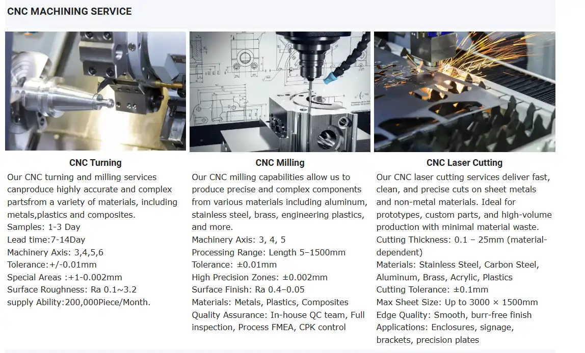
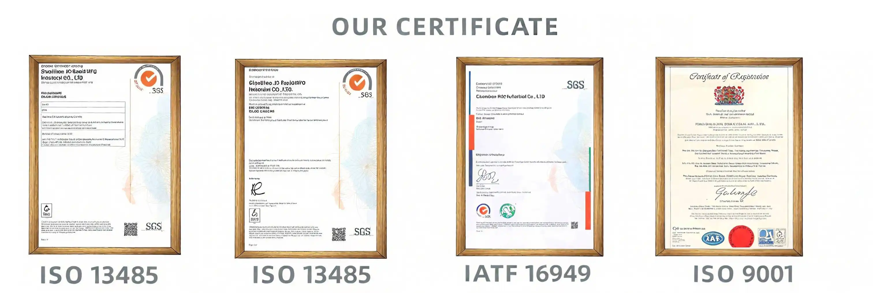
CNC (Computer Numerical Control) machining is a digitally-driven production method that uses pre-programmed software to control the movement of precise cutting tools on multiple axes. In semiconductor production, this method creates vital parts such as test socket housings, heat sink assemblies, and deposition chamber parts with micron-level precision. The process starts with CAD models being converted into G-code instructions that tell automated mills and lathes how to carve out complicated shapes from high-purity aluminium alloys (6061-T6, 7075), grades of stainless steel (316L, 304), titanium alloys, and high-performance polymers such as PEEK and POM. Dongguan Junsion Precision Hardware Co., Ltd. uses 32 CNC machines with ISO 9001:2015 certified processes to guarantee that all of our parts meet SEMI and RoHS requirements.
Traditional Machining Methods in Context
Conventional machining includes manual and semi-automated processes such as conventional milling, lathe turning, and surface grinding. This method relies on mechanical hand wheels and visible gauges to tune the cutting settings, which is prone to individual skill levels. These techniques worked well for less demanding applications decades ago, but they fail on the complex features needed in current semiconductor manufacturing, such as the micro-channels in plasma etching equipment or the perfectly aligned pin arrays in testing sockets. Without digital feedback loops, the dimensional drift builds during production runs. This results in batch discrepancies that endanger the dependability of the devices.
Operational Differences Impacting Production Quality
The main difference is the repeatability and scalability. A CNC system will repeat the same tool path a few thousand times. The walls will be the same thickness, the holes will be the same diameter, the surface will be the same flatness. Such conventional arrangements need manual recalibration between pieces, resulting in accumulated inaccuracies. CNC centers include automated tool changers, which may shift from drill to reamer to end mill in seconds. This allows multi-op workflows that would otherwise take many setups by hand. This efficiency immediately affects lead times, a vital consideration for procurement teams negotiating just-in-time delivery schedules with global OEMs and contract manufacturers of CNC Semiconductor Parts.
Limitations of Traditional Machining and the Emergence of CNC Technology
Tolerance Challenges in Conventional Processes
The tolerances of semiconductor parts are usually ±0.01mm to ±0.05mm, which are very hard to maintain manually in the batch manufacturing process. Traditional machining is frequently ±0.1mm at best, with the deviation increasing as the cutting tools wear. A case study from a communications equipment manufacturer showed that a move from manual milling to CNC machining of aluminium heat sink components decreased dimensional variance by 73%, directly enhancing thermal management efficiency in 5G base station modules. The failure to retain tight tolerances results in greater rejection rates in quality checks, which increases the per-unit cost even when the equipment cost is cheaper.
Geometric Complexity Limitations
The semiconductor industry increasingly demands parts with interior cavities, undercuts, and compound angles – characteristics that are difficult to fabricate effectively on typical three-axis manual machines. For instance, in the process of ion implantation, vacuum chamber parts such as those made by Junsion normally include complex gas flow channels and precisely angled mounting surfaces. CNC five-axis machining centers can dynamically rotate workpieces to access complicated geometries from a single setup, rather than requiring numerous manual operations and fixturing modifications. This ability eliminates the typical failure of conventional multi-stage production: the misalignment of processes.
Automation Solving Human Error Variables
Manual machining processes are plagued by human tiredness, misinterpretation of measurements, and irregular feed rates. Irregular pressure while grinding and incorrect depth adjustment might cause scrap bits that are only found in the final inspection. Closed-loop servo systems measure cutting forces in real-time and adjust speeds to minimise tool deflection, eliminating these factors in CNC automation. Uniform wall thickness is crucial for etching tool parts that can survive plasma corrosion, and programmed accuracy beats operator feel for this. Industries implementing CNC technology are seeing yields 15-30% higher than older techniques.
Core Evaluation Metrics for CNC vs Traditional Machining in Semiconductor Parts
Precision and Tolerance Capabilities
Dimensional precision is the name of the game for CNC Semiconductor Parts. For long production runs, CNC machining may achieve positional accuracies of ±0.005mm. In-process laser measuring devices validate measurements without removing parts from fixtures. The traditional approach is post-machining examination using micrometres and callipers, only detecting faults after material has been removed irrevocably. The difference is dramatic in the production of test socket components. A chip validation fails due to electrical contact failures caused by pin alignment inaccuracies of just 0.02mm. We consistently supply parts with ±0.01mm tolerances using temperature-controlled machining environments and tool wear compensation algorithms at our facilities.
Material Compatibility and Surface Finish Quality
Both techniques apply to common engineering materials, but CNC programming optimises cutting settings based on the individual machinability properties of each alloy. The work hardening behaviour of titanium alloys, which are widely used for corrosion-resistant semiconductor tools, is difficult to reliably control by human operators. The CNC machine uses variable helix end mills with high-pressure coolant (over 1000 PSI) to minimise heat buildup, something you can’t do with a manual machine. Surface finish requirements vary; vacuum chamber components need Ra values below 0.4 μm to avoid particle contamination, which may be obtained with CNC’s regulated feed rates and multi-pass finishing procedures that are not economically feasible with hand grinding.
Lead Time and Scalability Considerations
With CNC, changing programs is fast and easy. You may alter a dimension by changing a code, rather than retooling. A consumer electronics customer required 50 bespoke wafer handling components and weekly design revisions throughout product development. Using our CNC process, we were able to make these adjustments in 48-hour turnaround periods, while conventional machining would have required new fixtures and setup calibrations for each iteration. The benefits of CNC are even more significant when scaling up to production levels. Once a program is certified, executing 10 or 10,000 parts is the same with no process drift. Older techniques tend to show more variance when the operator fatigues over long runs; therefore, in-process inspections have to be frequent, reducing throughput.
Cost, Efficiency, and Supplier Considerations for CNC Semiconductor Parts
Economic Analysis Across Production Volumes
Initial CNC equipment investment exceeds traditional machinery costs, yet per-part economics favor automation at surprisingly low volumes. Setup costs in CNC operations concentrate in programming time (typically 2-4 hours for complex parts), after which lights-out manufacturing reduces labor expenses to near-zero. Traditional machining incurs recurring setup costs with each batch as operators reposition fixtures and verify tool offsets. Material waste also differs significantly—CNC's precise tool pathing minimizes excess removal, particularly valuable when machining expensive titanium or high-purity aluminum billets. A logistics storage equipment manufacturer saved 22% on material costs after switching heat sink production to CNC, despite higher hourly machine rates.
Evaluating Supplier Certifications and Capabilities
Procurement managers assessing semiconductor component suppliers should prioritize ISO 9001:2015 certification as baseline quality assurance, supplemented by industry-specific standards like SEMI S2 for equipment safety. Capability verification extends beyond certifications—request documentation of achievable tolerances, available machining envelope sizes, and surface treatment options. At Junsion, we maintain traceability through every production stage, from material certification (per ASTM B348 for titanium, AMS standards for aerospace-grade aluminum) through final dimensional reports generated by coordinate measuring machines. Responsiveness matters equally; suppliers with established CNC workflows typically quote within 24 hours and deliver prototypes in 5-7 days versus 2-3 weeks for traditional shops.
CNC Positioning Among Advanced Manufacturing Methods
While electrical discharge machining (EDM) excels at hardened materials and 3D printing enables rapid prototyping, CNC machining occupies the optimal space for CNC Semiconductor Parts requiring material properties and production volumes. EDM proves cost-prohibitive for aluminum components and suffers from slow material removal rates. Additive manufacturing introduces porosity concerns unsuitable for vacuum chamber applications demanding hermetic seals. Injection molding suits high-volume plastic components but cannot economically produce the low-to-mid volumes (50-5,000 units) typical in specialized semiconductor tooling. CNC bridges these gaps, offering material versatility, proven structural integrity, and economic scalability across the volume spectrum most procurement teams encounter.
Design and Manufacturing Best Practices for CNC Semiconductor Parts
Design-for-Manufacturability Principles
Close coordination between design engineers and production partners is critical to avoid expensive delays. Sharp interior corners induce stress concentration and need specific tooling. Specifying min radius values (usually 0.5mm for aluminium, 1.0mm for titanium) improves machinability, while retaining structural performance. Deep pocket features with high aspect ratios might result in tool deflection; therefore, talking to CNC professionals early in the design stage can help identify potential concerns before investing in tooling. We often evaluate customer CAD models to advise changes, such as increasing draft angles or moving important dimensions to more accessible surfaces, optimisations that may save machining time by 15-25% while maintaining functionality.
Material Selection Impact on Performance
The selection of stainless steel 316L and aluminium 6061-T6 for the etching tool components is based on a trade-off between corrosion resistance, heat conductivity, and weight. Stainless steel is tolerant to harsh plasma chemistries but has low thermal conductivity and may need active cooling. Aluminium is also great at dissipating thermal energy. However, it has to be anodised to guard against oxidation in reactive conditions. Chemically inert, electrically insulating high-performance polymers such as PEEK are good candidates for test socket housings where the use of metal would generate grounding problems. Our technical team will propose materials that are appropriate for your application specifics such as operating temperatures, chemical exposures, electrical requirements, and estimated service life to ensure maximum performance throughout the life of the component.
Addressing Micro-Tolerance and Thermal Management Challenges
The tolerances of ±0.02mm have to be controlled during machining, which means limiting thermal expansion. The heat generated during the cutting process causes the workpiece to increase temporarily. If you measure the pieces while they are still hot, they will contract below spec after they cool. We use temperature-stabilised machining conditions (20°C ±1°C) and heat dissipation times between roughing and finishing passes. Acoustic emission sensors monitor tool wear and sense dulling before it impacts dimensions, automatically changing tools. Tool life optimisation is needed in the manufacture of wafer handling components from aluminium 7075 because the hardness of this alloy increases the wear of the carbide, which has to be replaced often to maintain the sharpness of the edge and avoid a dimensional drift throughout the production batches.
Conclusion
CNC vs conventional machining of semiconductor parts has obvious benefits for computer-controlled automation. CNC technology removes the tolerance variations and scaling limits seen in manual processes, delivering the accuracy, repeatability and geometric flexibility that today’s electronics production requires. Traditional machining still has its niche in repair or very low volumes, but procurement professionals looking for reliable partners for wafer handling systems, etching equipment or thermal management assemblies will find CNC manufacturing offers better quality assurance, improved lead times and a better total cost of ownership. Partnering with vendors that have certified quality processes, sophisticated machining capabilities, and quick technical assistance can help guarantee your semiconductor parts fulfil the demanding criteria that fuel device dependability and manufacturing efficiency.
FAQ
1. What precision advantages do CNC processes offer over traditional machining?
CNC machining maintains tolerances within ±0.01mm across extended production runs through digitally controlled tool paths and real-time measurement feedback. Traditional methods rely on manual adjustments prone to operator variability, typically achieving ±0.1mm tolerances that prove insufficient for semiconductor applications requiring micron-level precision.
2. How do lead times compare between manufacturing approaches?
CNC programming allows rapid design iteration—dimension changes are implemented within hours rather than days. Prototype parts typically deliver in 5-7 business days, while traditional machining requires 2-3 weeks due to manual setup complexities. Production scaling favors CNC through lights-out manufacturing capabilities that maintain consistent output without operator intervention.
3. Can CNC handle customization for specialized semiconductor applications?
Advanced multi-axis CNC centers accommodate complex geometries including internal channels, compound angles, and undercuts common in vacuum chamber components and etching tool parts. Material compatibility spans high-purity aluminum alloys, corrosion-resistant stainless steels, titanium, and engineered plastics—all machinable with application-specific surface treatments like anodizing or electroless nickel plating to meet performance requirements.
Partner with Junsion for Superior CNC Semiconductor Parts Manufacturing
Dongguan Junsion Precision Hardware Co., Ltd. stands ready to support your precision component needs with ISO 9001:2015 certified quality systems and RoHS-compliant processes. As an established CNC Semiconductor Parts supplier serving electronics, communications, and consumer goods industries across 20+ countries, we combine advanced five-axis machining capabilities with responsive engineering support to deliver wafer handling components, etching tool parts, test socket assemblies, and thermal management solutions tailored to your specifications. Our 1,600 square-meter facility houses 32 CNC machines capable of maintaining ±0.01mm tolerances in materials ranging from aluminum 6061-T6 to titanium alloys and PEEK plastics. Contact our technical team at Lock@junsion.com.cn to discuss your project requirements and receive detailed quotations backed by our commitment to quality, punctual delivery, and long-term partnership. Let us demonstrate how precision manufacturing expertise translates into your competitive advantage.
References
1. Smith, J. R., & Anderson, M. K. (2021). Precision Machining for Semiconductor Manufacturing: Technology and Applications. Industrial Press.
2. Chen, L., Wang, H., & Liu, X. (2020). "Comparative Analysis of CNC and Conventional Machining in High-Precision Component Production," Journal of Manufacturing Science and Engineering, 142(8), 081005.
3. Thompson, R. D. (2022). Advanced CNC Machining: Techniques for Complex Geometries. McGraw-Hill Education.
4. Martinez, S., & O'Brien, P. (2019). "Quality Assurance in Semiconductor Equipment Manufacturing," Semiconductor International, 42(5), 34-41.
5. International Technology Roadmap for Semiconductors (2023). Manufacturing Equipment and Materials Requirements. Semiconductor Industry Association.
6. Zhang, Y., & Kumar, V. (2021). "Material Selection and Surface Treatment for Semiconductor Processing Equipment," Materials Science and Engineering Reports, 145, 100621.